This tutorial covers the steps involved in loading a bitstream into the Spartan 3E Evaluation Board for debugging and testing purpose. Two methods for loading bitstream are discussed here which are:
- Loading bitstream to the FPGA (Volatile)
- Loading bitstream to PROM (Non-Volatile)
Loading bitstream to FPGA
- Once the Generate Programming File process of the design implementation procedure completes successfully then the generated bitstream can be loaded into the development board. To initiate the loading process, double click on the Configure Target Device option, as shown in Figure 1 Box A. On doing so, a Warning dialog box appears that indicates that a new ISE iMPACT target configuration window will be opened. Click OK, as shown in Figure 1 Box B to continue.

Figure 1. Starting the ISE iMPACT program - When the ISE iMPACT window opens, then connect the Spartan 3E Evaluation Board to your PC via the USB cable.
- In the ISE iMPACT window, double click on the Boundary Scan button, as shown in Figure 2 Box A. The Boundary Scan connects to the development board through the in-built JTAG interface.

Figure 2. Starting the Boundary Scan of the target - When the Boundary Scan completes, the programmable components of the JTAG chain are read by ISE iMPACT. Upon the successful completion of Boundary Scan a new window opens with an option to initialize the JTAG chain, as shown in Figure 3 Box A.

Figure 3. Boundary Scan window - Right click on the Boundary Scan window and select Initialize Chain, as shown in Figure 4 Box A. This will initialize all the programmable components of the JTAG chain.

Figure 4. Initializing the JTAG chain - When the Initialize Chain process completes, then the programmable components of the development board are displayed, as shown in Figure 5 Box A,B and C. The components available in the Spartan 3E Evaluation Board are:
- xc3s400e(Box A) - FPGA
- xcf04s (Box B) - PROM
- xc2c64a (Box C) - CPLD

Figure 5. The programmable components of the JTAG chain - xc3s400e(Box A) - FPGA
- On clicking Yes, a new file open dialog box titled Assign New Configuration File opens. Navigate to the project directory. In this example the project directory is E:\My Work\Xilinx Projects\ANDgate. In the project directory, select the file with the same name as the project having a .bit extension. This is the bitstream file generated by the Generate Bitstream process. In this example the Bitstream file is andgate.bit. Select this file, as shown in Figure 6 Box A and click on Open, as shown in Figure 6 Box B to continue. On doing so the andgate.bit file is added to the FPGA device.

Figure 6. Assign New Configuration File dialog box for FPGA device - Next, another query dialog box appears which prompts whether or not to include an SPI or BPI PROM to the device. Click No, as shown in Figure 7 Box B to proceed.

Figure 7. Prompt to attach SPI or BPI PROM to target device - The configuration then proceeds to the PROM component of the JTAG chain. The Assign New Configuration File dialog opens again asking for the location of the .mcs file to load into the PROM. Since the PROM is not used in this form of FPGA loading, skip this step by clicking the Bypass button, as shown in Figure 8 Box A.

Figure 8. Assign New Configuration File dialog box for PROM device - The configuration continues for the final component in the chain, the CPLD. The Assign New Configuration File dialog then asks for the location of the file to load into the CPLD. The CPLD is not used in this method so skip this step by clicking the Bypass button, as shown in Figure 9 Box A.

Figure 9. Assign New Configuration File dialog box for CPLD device - This completes the configuration of all the programmable components in the JTAG chain of the Spartan 3E Evaluation Board. A new dialog box titled Device Programming Properties opens which lists all the programmable components and options for programming them. Select Device 1 (FPGA xc3s400e), as shown in Figure 10 Box A and Click OK to proceed.

Figure 10. Device Programming Properties dialog box with programming options for FPGA device - Now, the bitstream is ready to be loaded into the FPGA. Right click the FPGA device in the Boundary Scan window and click on Program, as shown in Figure 11 Box A.
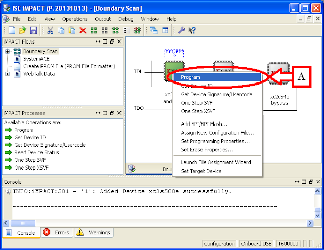
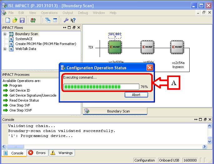
Figure 11. Programming the FPGA device - The Program process executes, as shown in Figure 12 Box A.

Figure 12. Program process being executed - Once the Program process is completed, the confirmation message is displayed in the Boundary Scan window, as shown in Figure 13 Box A.

Figure 13. Program process successful completion


Loading bitstream to PROM
- The procedure for loading bitstream to PROM is similar to that of loading bitstream to FPGA. After completion of the Generate Programming File process start the ISE iMPACT program by double clicking the Configure Target Device option, as shown in Figure 14 Box A. Click OK, as shown in Figure 14 Box B to acknowledge the warning presented in the Warning dialog box.

Figure 14. Starting the ISE iMPACT program - In the ISE iMPACT window, double click on the Create PROM File (PROM File Formatter) button to invoke the PROM File Formatter dialog box, as shown in Figure 15 Box A.

Figure 15. Launching the PROM File Formatter - In the PROM File Formatter dialog box, make sure that Xilinx FPGA/PROM is selected as the Storage Target, as shown in Figure 16 Box A and then click the arrow button, as shown in Figure 16 Box B to proceed.

Figure 16. PROM File Formatter select Storage Target step - Select the xcf04s device from the list of PROM devices, as shown in Figure 17 Box A.

Figure 17. PROM File Formatter select PROM storage device to add - Click on the Add Storage Device button, as shown in Figure 18 Box A to add the selected xcf04s device. The added device is listed in the box below, as shown in Figure 18 Box B. Verify that the device is correct and proceed to the next step by clicking the arrow button, as shown in Figure 18 Box C.

Figure 18. PROM File Formatter add PROM storage device - Next, select the destination path for the PROM file. To do so, click on the folder icon as shown in Figure 19 Box A. A Browse Folder dialog opens. In the Browse Folder dialog navigate to the project directory, which in this example is E:\My Work\Xilinx Projects\ANDgate. Select this folder as the destination path for the PROM file, as shown in Figure 19 Box B and click OK to proceed.

Figure 19. PROM File Formatter select destination path for PROM file - Upon completion of the PROM File Format selection, an Add Device dialog appears which prompts to start adding device configuration files to the PROM file. Click OK, as shown in Figure 20 Box A to start adding to the PROM file.

Figure 20. Prompt to start adding device configuration files to PROM file - A new Add Device file-open dialog opens. In this dialog navigate to the project directory, which in this example is E:\My Work\Xilinx Projects\ANDgate. Select the bitstream file which is the file having the same name as the project having a .bit extension. In this example, the bitstream file is andgate.bit which is selected as shown in Figure 21 Box A. Click on Open to add this file to the PROM file.

Figure 21. Bitstream file added to PROM file from the project directory - The Add Device dialog appears again and prompts to add other device configuration files to the PROM file. Click No, as shown in Figure 22 Box A to proceed.

Figure 22. Prompt to add more device configuration files to the PROM file - The Add Device dialog prompts that device configuration file adding procedure had completed. Click OK, as shown in Figure 23 Box A to proceed.

Figure 23. Prompt that indicates that device configuration file adding procedure has completed - Click on the Generate File button, as shown in Figure 24 Box A to generate the PROM file. Wait for the process to complete. When the process completes, a Generate Succeeded message is displayed, as shown in Figure 24 Box B.

Figure 24. PROM file generation - In the ISE iMPACT window, double click on the Boundary Scan button, as shown in Figure 25 Box A. The Boundary Scan connects to the development board through the in-built JTAG interface.

Figure 25. Starting the Boundary Scan of the target - When the Boundary Scan completes, the programmable components of the JTAG chain are read by ISE iMPACT. Upon the successful completion of Boundary Scan a new window opens with an option to initialize the JTAG chain, as shown in Figure 26 Box A.

Figure 26. Boundary Scan window - Right click on the Boundary Scan window and select Initialize Chain, as shown in Figure 27 Box A. This will initialize all the programmable components of the JTAG chain.

Figure 27. Initializing the JTAG chain - When the Initialize Chain process completes, then the programmable
components of the development board are displayed, as shown in Figure 28
Box A,B and C. The components available in the Spartan 3E Evaluation Board are:
- xc3s400e(Box A) - FPGA
- xcf04s (Box B) - PROM
- xc2c64a (Box C) - CPLD

Figure 28. The programmable components of the JTAG chain - xc3s400e(Box A) - FPGA
- On clicking Yes, a new file open dialog box titled Assign New Configuration File opens. Navigate to the project directory. In this example the project directory is E:\My Work\Xilinx Projects\ANDgate. In the project directory, select the file with the same name as the project having a .bit extension. This is the bitstream file generated by the Generate Bitstream process. In this example the Bitstream file is andgate.bit. Select this file, as shown in Figure 29 Box A and click on Open, as shown in Figure 29 Box B to continue. On doing so the andgate.bit file is added to the FPGA device.

Figure 29. Assign New Configuration File dialog box for FPGA device - Next, another query dialog box appears which prompts whether or not to include an SPI or BPI PROM to the device. Click No, as shown in Figure 30 Box B to proceed.

Figure 30. Prompt to attach SPI or BPI PROM to target device - The configuration then proceeds to the PROM component of the JTAG chain. The Assign New Configuration File dialog opens again asking for the location of the .mcs file to load into the PROM. Navigate to the project directory, which in this example is E:\My Work\Xilinx Projects\ANDgate. In the project directory, select the PROM file, which is the file having a .mcs extension. In this example, the PROM file is Untitled.mcs. Select this file, as shown in Figure 31 Box A and click Open, as shown in Figure 31 Box B to proceed.

Figure 31. Assign New Configuration File dialog box for PROM device - The configuration continues for the final component in the chain, the CPLD. The Assign New Configuration File dialog then asks for the location of the file to load into the CPLD. The CPLD is not used in this method so skip this step by clicking the Bypass button, as shown in Figure 32 Box A.

Figure 32. Assign New Configuration File dialog box for CPLD device - This completes the configuration of all the programmable components in the JTAG chain of the Spartan 3E Evaluation Board. A new dialog box titled Device Programming Properties opens which lists all the programmable components and options for programming them. Select Device 2 (PROM xcf04s), as shown in Figure 33 Box A. In the PROM Specific Properties, make sure that the Load FPGA option is selected, as shown in Figure 33 Box B. Click on OK, as shown in Figure 33 Box C to continue.

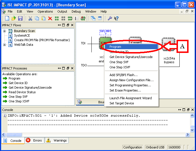
Figure 33. Device Programming Properties dialog box with programming options for PROM device - Right click the PROM device in the Boundary Scan window and click on Program, as shown in Figure 34 Box A.

Figure 34. Programming the PROM device - The Program process executes, as shown in Figure 35 Box A.

Figure 35. Program process being executed - Once the Program process is completed, the confirmation message is displayed in the Boundary Scan window, as shown in Figure 36 Box A.

Figure 36. Program process successful completion


