This is a quick take tutorial on how to get started with Xilinx ISE and the Spartan 3E Starter Board. The objective is to get the reader familiarized with the following steps:
- Creating a new Verilog project in Xilinx ISE
- Running simulation of the Verilog module using the ISIM simulator
- Implementing the project in a Spartan 3E Starter Board
Creating a new Verilog project in Xilinx ISE
- Launch Xilinx ISE 14.7 from the desktop shortcut icon as shown in the Figure 1.
 |
| Figure 1. Desktop Icon of Xilinx ISE 14.7 |
 |
| Figure 2. Xilinx ISE Launching |
- In the ISE Project Navigator window click on File in the menu bar as shown in Figure 3 Box A and then click New Project as shown in Figure 3 Box B to open the New Project Wizard.
 |
| Figure 3. ISE Project Navigator window and the File Menu |
- In the New Project Wizard's Create New Project window, perform the following three tasks:
 |
Figure 4. The New Project Wizard's Create New Project window
|
- Give a name to the project. Write the name of your project on the textbox marked Name as shown in Figure 4 Box A. In this example, the project name is ANDgate
- Select a Working Directory for the project. Click on the button in as shown in Figure 4 Box B to navigate through your hard drive. In this example, the project's Working Directory is E:\My_Work\Xilinx Projects\. and all the ISE files of the current project are stored in the project sub-folder E:\My_Work\Xilinx Projects\ANDgate.
- Select the top level source type for the project. Make sure the option HDL is selected as shown in Figure 4 Box C and then press Next to continue to the Project Settings window.
- In the Project Settings wizard, perform the following three tasks:
- Select a development board. In the Evaluation Development Board option, as shown in Figure 5 Box A, click on the button shown in Figure 5 Box B, which drops down to show a list of development boards supported by Xilinx ISE 14.7. Select the name of your development board. In this example, Spartan 3E Starter Board is selected as shown in Figure 5 Box C.
 |
| Figure 5. Project Setting window showing how to select development board |
Once the development board is selected the Family, Device, Package and Speed options for the board will automatically be updated as shown in Figure 6.
 |
| Figure 6. Family, Device, Package and Speed updated automatically after selecting development board. |
- Select the Simulator. In the Simulator option, as shown in Figure 7 Box A, click on the button shown in Figure 7 Box B, which drops down to show a list of simulators supported by Xilinx ISE 14.7. Select the simulator from the list. In this example, ISIM Simulator is selected as shown in Figure 6 Box C.
 |
| Figure 7. Project Setting window showing the selection of the ISIM Simulator |
- Select Preferred Language.In the Preferred Language option, as shown in Figure 8 Box A, click on the button shown in Figure 8 Box B, which drops down to show two options, VHDL or Verilog. In this example, Verilog is selected as the Preferred Language as shown in Figure 8 Box C.
 |
| Figure 8. Project Setting window showing selection of the Preferred Language (Verilog or VHDL) |
- Verify that the correct Evaluation Development Board, Simulator and Preferred Language are selected as shown in Figure 9 Box A and Box B and press Next to continue to the Project Summary window.
 |
| Figure 9. Project Setting window showing final values of all the options |
- In the Project Summary window all of the project settings selected so far are displayed. The Project Name, Project Path and Working Directory selected in step 3 are listed under Project: as shown in Figure 10 Box A. The Evaluation Development Board, Simulator and Preferred Language are listed under Device: as shown in Figure 10 Box B and C. Perform a final verification of all the settings and click on Finish to exit the New Project Wizard window.
 |
| Figure 9. Project Summary window showing all the selected settings |
- In the ISE Project Navigator's Design pane the project name and device ID for the newly created project are listed as shown in Figure 10 Box B. In this example, the name of the project is ANDgate and the device ID for the Spartan 3E is xc3s500e-4fg320.
 |
| Figure 10. The ISE Project Navigator window showing the name of the newly created project and the device ID of the target |
- In the ISE Project Navigator window click on Project in the menu bar as shown in Figure 11 Box A and then click New Project as shown in Figure 11 Box B to open the New Source Wizard to add a new Design Source File to the project. The Design Source File is the file in which the HDL definition of module defining the project is written.
 |
| Figure 11. ISE Project Navigator window and the Project Menu |
- In the New Source Wizard's Select Source Type window select Verilog Module as shown in Figure 12 Box A. Then, enter a name for this source file as shown in Figure 12 Box B. In this example, the source file is given the same name as the project: ANDgate. Click Next to continue to the Define Module window.
 |
| Figure 12. The New Source Wizard's Select Source Type window |
- In the Define Module window the Ports for the module can be defined. In the Port Name section shown in Figure 13 Box A write the name of the port. In the Direction section shown in Figure 13 Box B select whether the port is an input port, output port or inout (bidirectional) port. In the Bus section shown in Figure 13 Box C define the size of the port. To define a single-line port leave the checkbox under Bus un-checked. To define a multi-line port check the checkbox under Bus and define the number of lines by changing the values under MSB and LSB. It is more convenient to define ports in the source file editor so this step can be skipped. Click on Next to continue to the Summary window.
 |
| Figure 12. The New Source Wizard's Select Source Type window |
- In the Summary window verify the settings of the new Design Source File. Check the Source Name and Source Type of the new Design Source File before proceeding as shown in Figure 13 Box A. Click on Finish to exit the New Source Wizard.
 |
| Figure 13. The New Source Wizard's Summary window |
- In the ISE Project Navigator window the new Design Source File ANDgate.v is added to the project as shown in Figure 14 Box A and the source file is opened in the right pane of the Project Navigator. The newly created source file has definition comments and skeleton of Verilog module automatically inserted by the ISE as shown in Figure 14 Box C and D respectively. In the Design pane the source file is preceded by a symbol as shown in Figure 14 Box B which designates this source file as the file containing the top module (the main module defining the project).
 |
| Figure 14. The ISE Project Navigator window showing the contents of the newly created Design Source File |
- In the Source File,(if step 10 skipped) inside the parenthesis() of module list out the ports that are required in your design as shown in Figure 15 Box A. Then define the direction(input, output or inout) and size of the ports as shown in Figure 15 Box B. In this example, sigIn1 and sigIn2 are defined as the two input ports and sigOut as the output port of a 2-input AND gate. Since the ports are single-line there is no size parameter in the definition of the ports.
After declaring and defining the ports of the module, define the function that the module will carry out. The module function can be modeled using Combinational logic, Sequential logic or as a Finite State Machine(FSM). In this example, the module is modeled using Combinational logic as shown in Figure 15 Box C. The Combinational logic assign statement assigns the result of the ANDing of input ports sigIn1 and sigIn2 to the output port sigOut.
 |
| Figure 15. Defining the module |
- Save the source file after defining all the ports and functions. The ISE checks for syntax errors in the code while saving. The errors and/or warnings that the ISE finds while checking the source are listed in the Error and Warnings panes as shown in Figure 16 Box A. If there are no syntax errors then the source file is saved and the message Parsing design hierarchy completed successfully is displayed in the Console pane as shown in Figure 16 Box B.
 |
| Figure 16. The Console pane when saving a Design Source File |
- The source file now needs to be synthesized to check whether the defined module can be implemented as a unit of hardware or not. To do so select the source file in the Implementation tab of the Design pane as shown in Figure 17 Box A and double-click on Synthesize - XST as shown in Figure 17 Box B. Watch the Errors and Warnings pane for errors during the synthesis process. If no errors occur then the Console pane will display the message Process "Synthesize - XST" completed successfully as shown in Figure 17 Box C.
 |
| Figure 17. The Synthesize process |
Running simulation of the Verilog module using the ISIM simulator
- In the ISE Project Navigator window click on Project in the menu bar as shown in Figure 18 Box A and then click New Project as shown in Figure 18 Box B to open the New Source Wizard to add a new Simulation Source File to the project. The Simulation Source File is the file used to test the project module defined in the Design Source File.
 |
| Figure 18. ISE Project Navigator window and the Project Menu |
- In the New Source Wizard's Select Source Type window select Verilog Text Fixture as shown in Figure 19 Box A. Then, enter a name for this source file as shown in Figure 19 Box B. In this example, the source file is given the name: ANDgate_tb to indicate that this Simulation Source File is associated with the design source ANDgate.v. Click Next to continue to the Associate Source window.
 |
| Figure 19. The New Source Wizard's Select Source Type window |
- In the Associate Source window select the from a list of design sources the design source which this simulation source is associated with. In this example, the project has only one design source so that source is selected as shown in Figure 20 Box A. Click on Next to continue to the Summary window.
 |
| Figure 20. The New Source Wizard's Associate Source window |
- In the Summary window verify the settings of the new source file. Check the Source Name and Association of the new source file before proceeding as shown in Figure 21 Box A. Click on Finish to exit the New Source Wizard.
 |
| Figure 21. The New Source Wizard's Summary window |
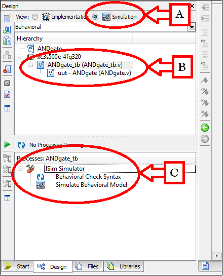
- In the Simulation tab of the Design pane, shown in Figure 22 Box A, the newly created simulation source is added to the project as shown in Figure 22 Box B. The simulation source file sits at the top of the hierarchy and under it is the design source file under test. The processes to invoke the ISIM simulator is also present under the Simulation tab as shown in Figure 22 Box C.
 |
| Figure 22. The Project Navigator's Design pane showing the how the newly created Simulation Source File sits in the Project Hierarchy |
- The ISE automatically fills up the newly created Simulation Source File with a skeleton of Verilog simulation code. All the sections shown in Figure 23 are generated by the ISE. This Simulation Source controls the inputs to and monitors the outputs from an instance of the Design Source and checks whether or not the designed behavior matches with the desired behavior. In this example, the instance of the designed module is called with an instance name uut as shown in the Figure 23 Box B. The input and output lines to this instance are defined as shown in Figure 23 Box A and a set of controlled inputs are fed to the instance using the initial block. The ISE initializes the input lines to 0 as shown in Figure 23 Box C. A sequence of controlled inputs have to be written in the space under Add stimulus here section marked in Figure 23 by Box D to test the designed module.
 |
| Figure 23. The contents of the Simulation Source File |
- Add a set of control inputs to the initial block as shown in Figure 24 Box A. In this example, the four possible combinations of the inputs sigIn1 and sigIn2 are fed into the instance uut of the designed module with a delay between each input combintaion of 20ns(#20;).
 |
| Figure 24. The set of control inputs defined in the Simulation Source File |
- After adding the control inputs, save the Simulation Source File. The ISE also checks this file for syntax errors while saving. If there are no errors in syntax then the message Parsing design hierarchy completed successfully is displayed as shown in Figure 25 Box A in the Console pane. Double click on the Behavioral Check Syntax process under Isim Simulator in the Simulation tab of the Design pane as shown in Figure 25 Box C. This process also parses the project source files to find syntax errors.
 |
| Figure 25. The Console pane when saving a Simulation Source File |
- When the Behavioral Check Syntax process is completed and no syntax errors are detected, the message Process "Behavioral Check Syntax" completed successfully is displayed in the Console pane as shown in Figure 26 Box A. Now, double click on the Simulate Behavioral Model to start the simulation of the designed module in a new ISIM Simulator window as shown in Figure 26 Box C.
 |
| Figure 26. The Console pane when Behavioral Check Syntax process completes |
- In the ISIM Simulator window, a Simulation Frame showing the input and output signal waveforms from the designed module are plotted as shown in Figure 27. The ISIM Simulator by default plots the Simulation Frame for a duration of 1 us as shown in Figure 27 Box A. To navigate to the start of the frame press the button shown in Figure 27 Box B.
 |
| Figure 27. The ISIM Simulator window showing the end section of the Simulation Frame |
- At the start of the Simulation Frame, there is a duration of 100ns, marked in Figure 28 as Box A, where the inputs to the designed module are zero. This is due to the delay statement #100; in the initial block of the Simulation Source File. After this delay, the control inputs are fed one by one to the designed module. Each set of control inputs is held for a duration of 20ns. The set of control inputs are marked in Figure 28 as Box B, Box C, Box D and Box E. At each of these states, the designed module has generated the correct result which means that the designed behavior matches the desired behavior.
 |
| Figure 28. The ISIM Simulator window showing the start section of the Simulation Frame |
Implementing the project in a Spartan 3E Starter Board
- In the ISE Project Navigator window click on Project in the menu bar as shown in Figure 29 Box A and then click New Project as shown in Figure 29 Box B to open the New Source Wizard to add a new Implementation Constraints File to the project. The Implementation Constraints File is used to map the ports of the designed module to the actual pinouts of the FPGA.
 |
| Figure 29. ISE Project Navigator window and the Project Menu |
- In the New Source Wizard's Select Source Type window select Implementation Constraints File as shown in Figure 30 Box A. Then, enter a name for this source file as shown in Figure 30 Box B. In this example, the source file is given the name ANDgate_ucf to indicate that this Implementation Constraints File is associated with the design source ANDgate.v. Click Next to continue to the Summary window.
 |
| Figure 30. The New Source Wizard's Select Source Type window |
- In the Summary window verify the settings of the new source file. Check the Source Name of the new source file before proceeding as shown in Figure 21 Box A. Click on Finish to exit the New Source Wizard.
 |
| Figure 31. The New Source Wizard's Summary window |
- In this example, the input lines sigIn1 and sigIn2 are mapped to two slide switches and the output line sigOut is mapped to an LED on the development board. To find pin associations for the Spartan 3E Starter Board, consult the Example User Constraints File chapter in the Spartan 3E Starter Board User Guide(UG230). A snippet of the chapter is shown in Figure 32.
 |
| Figure 32. Examples of Implementation Constraints mapping |
- Copy the constraints definition of two slide switches and one LED from the user guide to the Implementation Constraints File ANDgate_ucf as shown in Figure 33 Box A.
 |
| Figure 33. Constraints definition copied to the Implementation Constraints File |
- Change the NET values in the copied constraints definitions to the names of the ports of the designed module as shown in Figure 34 Box A. Do not change the other parameters in the constraints definition.
 |
| Figure 34. Constraints definition NET list changed to port names of the designed module |
- In the Implementation tab of the Design pane in the Project Navigator window, double click on the Generate Programming File process. The Implement Design and Generate Programming File processes will execute, and when they are completed, the message Process "Generate Programming File" completed successfully is displayed in the Console pane as shown in Figure 35 Box D. When all the processes shown in Figure 35 Box C are completed properly then the designed module is ready to be programmed into the development board.
 |
| Figure 35. The Console pane when Implement Design and Generate Programming File processes complete |