-
Introduction
Memory is a basic element in any system whether the memory is volatile or non-volatile. In this example, a volatile memory unit is designed in the form of a Synchronous Static RAM. Static Random-Access Memory (SRAM) is a type of semiconductor memory that uses bi-stable latching circuitry to store each bit. The term Static differentiates it from Dynamic RAM (DRAM) which must be periodically refreshed. SRAM retains data, but it is still volatile as data is lost when the power to the memory unit is cut off. -
Verilog Module
Figure 1 presents the Verilog module of the Synchronous SRAM. This Synchronous SRAM can store eight 8-bit values. The Synchronous SRAM module consists of a 8-bit data input line, dataIn and a 8-bit data output line, dataOut. The module uses an 8-bit address line, Addr to locate the position of data-byte within the memory array. With an 8-bit address line a 256-unit deep SRAM can be addressed, but in this example, an 8-unit deep SRAM is designed for simplicity. The module is clocked using the 1-bit input clock line Clk. The module also has a 1-bit chip select line, CS.
The 1-bit RD line is used to signal a data read operation on the Synchronous SRAM and the 1-bit WE line is used to signal a data write operation on the Synchronous SRAM. Both the RD and WE lines are active high.

Figure 1. Verilog module of Synchronous SRAM -
Verilog Code for Synchronous SRAM (syncRAM.v)
- module syncRAM( dataIn,
- dataOut,
- Addr,
- CS,
- WE,
- RD,
- Clk
- );
- // parameters for the width
- parameter ADR = 8;
- parameter DAT = 8;
- parameter DPTH = 8;
- //ports
- input [DAT-1:0] dataIn;
- output reg [DAT-1:0] dataOut;
- input [ADR-1:0] Addr;
- input CS,
- WE,
- RD,
- Clk;
- //internal variables
- reg [DAT-1:0] SRAM [DPTH-1:0];
- always @ (posedge Clk)
- begin
- if (CS == 1'b1) begin
- if (WE == 1'b1 && RD == 1'b0) begin
- SRAM [Addr] = dataIn;
- end
- else if (RD == 1'b1 && WE == 1'b0) begin
- dataOut = SRAM [Addr];
- end
- else;
- end
- else;
- end
- endmodule
Figure 2. Verilog Code for Synchronous SRAM -
Verilog Test Bench for Synchronous SRAM (syncRAM_tb.v)
- `timescale 1ns / 1ps
- module syncRAM_tb;
- // Inputs
- reg [7:0] dataIn;
- reg [7:0] Addr;
- reg CS;
- reg WE;
- reg RD;
- reg Clk;
- // Outputs
- wire [7:0] dataOut;
- // Instantiate the Unit Under Test (UUT)
- syncRAM uut (
- .dataIn(dataIn),
- .dataOut(dataOut),
- .Addr(Addr),
- .CS(CS),
- .WE(WE),
- .RD(RD),
- .Clk(Clk)
- );
- initial begin
- // Initialize Inputs
- dataIn = 8'h0;
- Addr = 8'h0;
- CS = 1'b0;
- WE = 1'b0;
- RD = 1'b0;
- Clk = 1'b0;
- // Wait 100 ns for global reset to finish
- #100;
- // Add stimulus here
- dataIn = 8'h0;
- Addr = 8'h0;
- CS = 1'b1;
- WE = 1'b1;
- RD = 1'b0;
- #20;
- dataIn = 8'h0;
- Addr = 8'h0;
- #20;
- dataIn = 8'h1;
- Addr = 8'h1;
- #20;
- dataIn = 8'h10;
- Addr = 8'h2;
- #20;
- dataIn = 8'h6;
- Addr = 8'h3;
- #20;
- dataIn = 8'h12;
- Addr = 8'h4;
- #40;
- Addr = 8'h0;
- WE = 1'b0;
- RD = 1'b1;
- #20;
- Addr = 8'h1;
- #20;
- Addr = 8'h2;
- #20;
- Addr = 8'h3;
- #20;
- Addr = 8'h4;
- end
- always #10 Clk = ~Clk;
- endmodule
Figure 3. Verilog Test-bench for Synchronous SRAM -
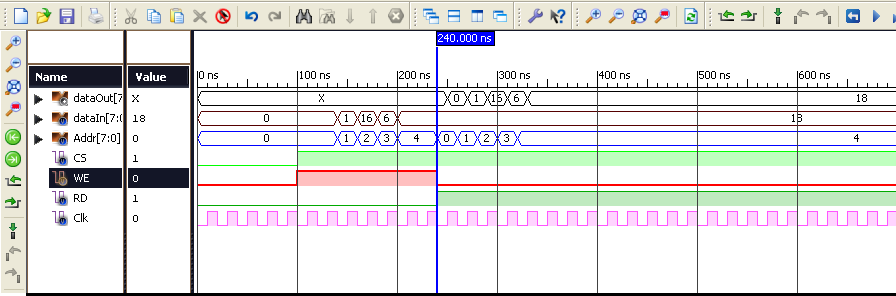
Timing Diagram
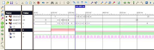
Figure 4. Timing diagram of Synchronous SRAM with four data
Synchronous Static RAM

Subscribe to:
Posts (Atom)